

Semiconductor cleanroom manufacturer
Semiconductor cleanrooms, where one stray particle is one lost device
Fabtech is the Indian manufacturer that designs, builds and validates semiconductor cleanrooms in-house, ISO Class 3 to 7, end to end. One stray particle scraps a finished wafer, so we build rooms that keep out what you cannot see: the dust, the chemical fumes in the air, and even the tremor in the floor.
Tell us what you make and how clean the process has to be. The engineers who would design the room will work the specification out with you.
- ISO Class 3 to 7
- FFU ceilings, built in-house
- ULPA U15 to U17
- AMC control
- ESD-protected areas
2,000+ controlled environments delivered across every industry that needs controlled air since 2004. One accountable engineering team designs, builds and validates the room. ISO Class 3 to 7. Semiconductor cleanroom solutions in India, from the first design to the validation dossier.
The room a wafer needs
A semiconductor cleanroom is an ultra-low-particle, ESD- and contamination-controlled room where wafers and devices are fabricated, assembled and tested. Most of them run at ISO 14644 Class 3 to 7. Fan-filter-unit ceilings with HEPA and ULPA filtration, steady temperature and humidity, and a low-vibration build are what hold that class.
- ISO 14644
- ISO Class 3 to 7
- HEPA H14
- ULPA U15 to U17
- FFU
- AMC
- ACPH
The reason is scale. Feature sizes are now measured in nanometres, so a speck of dust you cannot see is larger than the circuit it lands on.
At a glance
- Typical class
- ISO 14644 Class 3 to 7
- Ceiling
- Fan filter units, built in-house
- Terminal filtration
- HEPA H14 to ULPA U17
- Also controlled
- AMC, ESD, temperature, RH, vibration
- Classified to
- ISO 14644-1, -2 and -3
- Delivered by
- One team, design to validation
In semiconductors, cleanliness is yield
Every fab is judged on one number. How many working chips come off each wafer. Contamination is what pulls that number down. It is not a cosmetic problem. It is scrapped product. Preventing that is the whole job of the room.
Everything else follows from it. A defect let in early rides through every later step, so the wafer keeps absorbing cost long after the die is already dead. The cleaner and steadier the room, the more good die come off the line. That is why a clean room for the semiconductor industry is held to stricter limits than almost any other field.
Yield
The one number every fab is judged on
We engineer for exactly that.
- ParticlesIt starts with ISO Class 3 to 7 rooms under dense fan-filter ceilings. The most sensitive zones carry terminal HEPA and ULPA filters.
- Air-change rateAir-change rates run high and stay steady, because a class held only at rest is not a class held in production.
- StaticFloors and surfaces that will not hold a static charge, grounded and verified as ESD-protected areas.
- Temperature and humidityTemperature and humidity that barely move, for process repeatability and for static control alike.
- Molecules and vibrationChemical filtration for the fumes that particle filters miss. And a structure that stays still, because the tools that print and measure the circuits cannot tolerate a tremor.
Classification and semiconductor clean room standards
The class a fab zone is held to is set by the step it protects, not by the size of the building. These are the classes we build across, with the filtration and the control that holds each one.
Each rung on the ladder is a factor of ten. ISO Class 3 is four decades cleaner than ISO Class 7, not four steps.
FIG. 01ISO 14644-1:2015 airborne particulate classes across a semiconductor fab. Each figure is the maximum permitted concentration of particles 0.5 micron and larger per cubic metre, on a logarithmic axis, so every rung is a factor of ten. Filter grades are EN 1822 designations for the terminal stage over that zone.
| ISO 14644-1 class | Where it fits in a fab | Filtration and key controlTHIS PAGE |
|---|---|---|
| ISO Class 3 to 4 | Most sensitive lithography and wafer steps | ULPA U15 to U17, near-full FFU ceiling, AMC chemical filtration |
| ISO Class 5 | Wafer fabrication and critical process zones | Unidirectional flow, HEPA H14 and ULPA, tight RH and vibration limits |
| ISO Class 6 | Broader fabrication and process support | HEPA H14, high ACPH, ESD control |
| ISO Class 6 to 7 | Back-end assembly, bonding, packaging and test | HEPA H13 and H14 with an ESD-protected area (EPA) |
FIG. 02Classes per ISO 14644-1:2015. Filtration grades per EN 1822.
The rule of thumb: the more sensitive the step, the cleaner the room, and the more of the ceiling has to be filter. The wafer and lithography steps that decide a device sit at the tight end of the scale. Broader fabrication, assembly and test sit further down it.
Semiconductor clean room standards come from one international series, written in three parts. Each part settles a different question. The older American system that fabs once quoted has been retired.
| Standard | What it settles |
|---|---|
| ISO 14644-1 | The particle classes themselves, and how a room is classified against them |
| ISO 14644-2 | The monitoring that keeps a room inside its class after handover |
| ISO 14644-3 | The test methods used to prove both |
| Federal Standard 209E (retired) | The old Class 1, 10 and 100 fab ratings, superseded by ISO 14644 in 2001 |
FIG. 03ISO 14644 parts 1 to 3. Federal Standard 209E was cancelled in 2001.
If a legacy spec or an old tender still quotes those retired numbers, we simply map them onto the current classes. For the full class-by-class breakdown, see our cleanroom classification overview.
Every class, side by side
The full ISO 14644-1 table, the EU-GMP grades beside it and the legacy Class 100 mapping live on one reference page.
AMC control, FFU ceilings and ULPA filtration
Particle filters alone do not make a fab clean. At nanometre scale, two invisible threats matter just as much: chemical fumes in the air, and the tiniest building tremor. A trace of acid or ammonia gas can fog a photoresist or corrode a wafer surface long before any particle lands.
A vibration you would never feel can blur a lithography exposure. Semiconductor cleanroom technology is the engineering that controls all three threats at once. This is where high tech semiconductor cleanrooms part company with ordinary controlled space.
Three systems carry that load, and each is sized to the process it protects:
Particles only
What a HEPA or ULPA filter removes
| System | What it does | Engineering detailTHIS PAGE |
|---|---|---|
| Fan-filter-unit (FFU) ceilings | Push a steady curtain of clean air down through the room | Near-unidirectional flow, high ACPH, terminal HEPA H14 and ULPA U15 to U17 sized to the ISO class |
| AMC (airborne molecular contamination) control | Strips the gases that particle filters cannot touch | Gas-phase chemical filtration: activated-carbon and chemisorption media for acids, bases (ammonia), condensables and dopants, media grade matched to the process (scope confirmed per project on request) |
| Vibration and thermal stability | Keeps exposures sharp and measurements true | Low-vibration structural design and isolation for litho and metrology tools; temperature and RH held in tight bands for repeatability and ESD safety |
FIG. 04Filtration grades per EN 1822. Media grade is matched to the process.
Worth pinning to the wall: HEPA and ULPA filters remove particles only, never gases. Molecular contamination needs its own chemical filtration stage.
Under EN 1822 a HEPA H14 filter removes at least 99.995 percent of particles at MPPS, the most penetrating particle size, and a ULPA U15 at least 99.9995 percent. Grade selection is by zone, not by room, which is why one fab can carry three grades at once.
The ceiling is ours
We manufacture the fan filter units and the terminal HEPA and ULPA housings that make up that ceiling, so the grid that holds the class is engineered by the team that installs it.
One naming note, because two things share an acronym on this site. Here, AMC means airborne molecular contamination. Any equipment maintenance contract we mention elsewhere is separate, and scoped to equipment only.
Where in the line a defect costs most
In a fab, cleanliness has a number attached to it. Each wafer carries hundreds or thousands of potential devices. Every defect removes good die and pushes up the cost of the ones that survive. A particle, a chemical trace, a vibration-blurred exposure: each takes its bite.
Every step
adds value that a late defect destroys
Timing matters as much as count. Value is added at every step, so an early defect wastes every step that comes after it, while a late one destroys the value of every step that came before. Either way the room has to hold at all of them. The room specification is therefore driven backward from yield, never chosen by habit.
How to read the map below
Each square is one die site. A particle at or above the critical defect size turns its die dark and the good-die count drops with it. A smaller hit lands and the die lives. Watch both wafers at once: the coarser air loses die faster at every point in the cycle, and the curve underneath says why.
Air at ISO Class 6
D = 0.35 per sq cm
HEPA H14 ceiling, partial filter coverage
Good die
of 112 die sites
Die 10 mm x 10 mm, 1 sq cm / critical defect 45 nm / 33 scrapped, 22 sub-critical hits survived
Air at ISO Class 4
D = 0.10 per sq cm
ULPA U15 ceiling, near-full coverage, AMC stage
Good die
of 112 die sites
Die 10 mm x 10 mm, 1 sq cm / critical defect 45 nm / 11 scrapped, 8 sub-critical hits survived
- Live die
- Scrapped die
- Critical defect, at or above 45 nm
- Sub-critical hit, the die lives
FIG. 05Two wafers, same die size, different air. Particles land, a hit at or above the critical defect size scraps that die, and the good-die count falls with it. Illustrative Poisson model (yield equals e to the power of minus defect density times die area, at a 1 sq cm die), not a yield prediction for any process: the ISO class shown against each defect density is the air that makes that density achievable, not a published conversion between the two.
The defect density a process can tolerate sets the class, the FFU coverage, the AMC filtration grade, and the humidity and vibration limits. Each of those settings changes how many good devices survive that step.
So we design the room around its most sensitive operation. Then we prove it. Particle counts and environmental mapping measure the room. HEPA and ULPA integrity tests prove the filters. The cleanliness that protects yield on paper becomes the cleanliness proven on test day.
What a semiconductor cleanroom must deliver
Semiconductor cleanroom systems make five promises. Here is the engineering that keeps each one.
Particle class matched to yield
A cleaner room means fewer defects, so the class is set by the most sensitive step the room must hold.
AMC (airborne molecular contamination) control
Invisible fumes ruin wafers too. The air is scrubbed of gases as well as particles.
ESD control everywhere
A discharge too small to feel can puncture a gate oxide on a wafer, or kill a finished device during back-end assembly.
Environmental and vibration stability
The room must read identical all shift, every shift.
Cleanable, low-outgassing build
Surfaces that stay clean, do not shed and wipe down fast.
And the numbers behind those promises:
FIG. 06, below
| Promise | Engineering detail |
|---|---|
| Particle class | ISO Class 3 to 7 per ISO 14644-1: most-sensitive fab steps toward ISO 3 to 5, back-end assembly and test to ISO 6 to 7, FFU-dense ceilings with a high filter-coverage ratio, terminal HEPA H14 and ULPA U15 to U17 over critical zones |
| AMC control | Gas-phase chemical filtration (activated-carbon and chemisorption) for acids, ammonia, condensables and dopants, the contamination particle filters miss |
| ESD control | ESD-protected areas (EPA) on the back-end assembly and test floor: ESD-dissipative epoxy and PU flooring, grounded antistatic surfaces, controlled humidity holding device- and wafer-level static in a safe band |
| Stability | Tight temperature and RH bands, high stable ACPH, pressure cascade, low-vibration design for metrology and litho |
| Build | In-house modular wall and ceiling systems on PUF and Rockwool panels, with honeycomb-infill panels available where a project calls for them, flush detailing, seamless ESD flooring and low-particle-generating materials |
FIG. 06Classes per ISO 14644-1. Filter grades per EN 1822.
HVAC and heat-load management for semiconductor fabs
Two things make semiconductor air the hardest we condition. First, the cleanliness: these rooms turn their air over faster, through more filter, than anything else we build. Second, the heat: a fab packs dense process and tool heat into a sealed space.
That heat has to be removed without disturbing the very airflow that keeps the room clean. Get the HVAC wrong and you lose the class, the stability, or both.
A semiconductor cleanroom HVAC system pairs fan-filter-unit ceiling grids with make-up air units (MAU). Terminal HEPA and ULPA stages plus chemical AMC filtration clean the supply air. Air-change rates are sized to the class. The cooling and return-air strategy then carries the process heat load out without upsetting the downward flow or the pressure balance between rooms.
Temperature and humidity hold tight bands, for process repeatability and for ESD control. The whole system is proven by HVAC validation before you take the room over. That proof runs as part of OQ and PQ.
In our own facility
The air-handling units and the make-up air units are built in our own facility, alongside the FFUs and the terminal filter housings, so the air path is one company's engineering from the coil to the ceiling.
- Fab zones we engineer
- ISO Class 3 to 7
- Terminal grade over critical zones
- ULPA U15 to U17
- Gas-phase chemical filtration stage
- AMC
- Protected areas on the back-end floor
- ESD (EPA)
How a semiconductor fab cleanroom is built
A semiconductor cleanroom design starts from the process, not the floor plan. We capture the user requirement specification (URS) and the yield-critical class for each operation. Then the airflow, the filter layout, the AMC strategy, the ESD regime and the vibration plan resolve into one coordinated design. From there it is one accountable, six-stage flow:
One team
carries every stage below
| Stage | What happens | RecordTHIS PAGE |
|---|---|---|
| 01Requirements and class target | The defect tolerance and the tool list for each zone set the ISO class the room must hold. | URS |
| 02Design and DQ | Airflow and filter coverage, AMC filtration, ESD and vibration strategy, and the pressure cascade between rooms, resolved and frozen. | DQ |
| 03In-house manufacture and factory testing | The modular envelope and the equipment are built in our own facility and tested before dispatch. | FAT, equipment only |
| 04Installation and IQ | Envelope, filter ceilings, flooring and services go in, and every install is inspected. | IQ |
| 05Commissioning, OQ and PQ | Filter integrity on the HEPA and ULPA stages, airflow uniformity, recovery and pressure mapping. Particle-count certification to the room's class. | OQ, PQ, ISO 14644-1 |
| 06Handover | As-builts, the validation dossier and the equipment maintenance contract. Ongoing facility upkeep stays client-managed. | As-builts and dossier |
FIG. 07FAT covers equipment only. Ongoing facility upkeep stays client-managed.
Nothing in that list changes hands. The engineers who set the class are the engineers who sign the particle count, which is the whole reason the stages read as one flow rather than as six handovers.
Where the stage detail lives
Semiconductor applications we engineer for
Seven kinds of room, from the lithography bay that decides a device to the test floor that ships it.
Wafer fabrication and process steps
This is the cleanroom semiconductor fabrication core. Deposition, etch, diffusion, and the litho support that needs the lowest class and AMC control.
Photolithography support
Vibration- and AMC-sensitive zones around the exposure tools.
Microelectronics and chip packaging
Assembly, bonding and encapsulation in ESD-protected areas.
Assembly, bonding and test
Back-end ISO 6 to 7 cleanrooms with full ESD protection for finished-device handling.
Metrology and inspection rooms
Low-vibration, stable-environment rooms for measurement tools.
Photonics and compound-semiconductor work
Specialised process and handling environments.
R&D and pilot lines
Flexible, validated rooms that scale a process from lab to production.
For battery, PCB and SMT and broader electronics-assembly cleanrooms, see our electronics manufacturing cleanrooms. For pharma-grade controlled environments, see pharmaceutical cleanrooms.
Semiconductor cleanroom room types we build
A clean room in semiconductor manufacturing is rarely one room. It is a set of them, each doing a different job.
- Wafer-process and fabrication cleanrooms
- ESD-protected assembly and packaging areas (EPA)
- Test and metrology rooms
- Gowning and air-shower entries
- Pass-box and material-transfer staging
Each room is designed for the particle class, the AMC and ESD regime, and the vibration limits its operation demands. Together they have to behave as one system, not as a set of separate rooms. That is what semiconductor cleanroom infrastructure means.
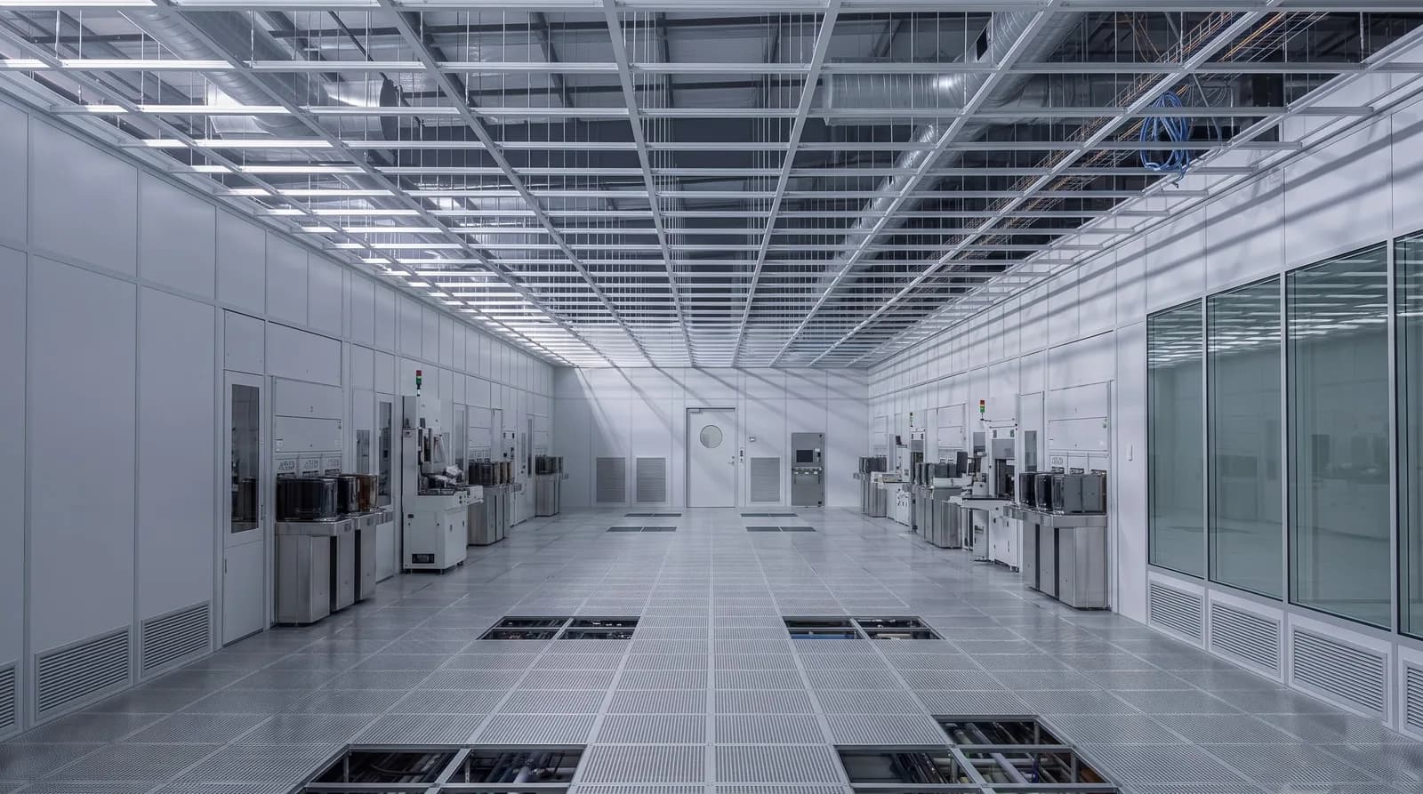
A fan-filter-unit ceiling is the defining feature of a fab. The grid, its terminal housings and the units themselves are built in our own facility.
Validation, documentation and compliance
We don't just claim the class. We prove it on test day, and hand you the evidence. Every stage is run and documented before you take the room over.
Design qualification (DQ) locks the engineering. Installation qualification (IQ) verifies what was built. Operational qualification (OQ) proves the systems run as designed. Performance qualification (PQ) proves the room performs in use.
The tests behind those letters:
What you take away
The dossier is packaged for your quality and process-engineering teams. And the room is built to stand inspection under the standards your customers audit to.
| Test on the day | What it proves |
|---|---|
| HEPA and ULPA filter integrity (PAO or DOP) | No leaks through or around a terminal filter |
| Airflow velocity and uniformity | The ceiling delivers even, stable downward flow |
| Recovery testing | The room returns to class quickly after a disturbance |
| Pressure mapping | Room-to-room pressure relationships hold as designed |
| Particle-count certification to ISO 14644-1, -2 and -3 | The room meets its class on the meter, not just on paper |
| ESD verification of flooring and surfaces | Static control performs where it is specified |
| AMC filtration checks (where specified) | The chemical filtration stage performs as designed |
FIG. 08Particle-count certification per ISO 14644-1, -2 and -3.
Why Fabtech for a semiconductor cleanroom
You are dealing with one accountable engineering team. Fabtech Cleanrooms is the semiconductor cleanroom manufacturer that owns your room from first design to final handover. There is no chain of subcontractors to pass blame down when a number drifts. One company answers for the class, and it is the company that built the room.
Under that single point of accountability sits the full engineering range. ISO Class 3 to 7 capability, with AMC, ESD and vibration control. We manufacture in-house and engineer the FFU ceilings ourselves. The HEPA and ULPA filtration is sized to the process it protects. Delivery is validated and documented to the ISO class your auditors read.
One semiconductor cleanroom supplier for the room, the equipment and the paperwork.
The specification a fab conversation starts from
Two of these numbers mark the ends of the range we build to. The other two are the delivered record behind it, counted since 2004. None of them replaces the class your own process sets.
- Lowest class we build toISO 14644-1, litho and wafer steps
- ISO 3
- Highest ULPA grade specifiedEN 1822, most sensitive zones
- U17
- Controlled environments deliveredDesign, build and validation
- 2,000+
- Sector served since 2004Semiconductor among them
- Any
Semiconductor cleanrooms, common questions
A tightly controlled, ultra-low-particle environment where semiconductor devices are fabricated, assembled and tested, usually at ISO Class 3 to 7. Contamination at nanometre scale causes defects and lost yield. So the room controls particles, static, airborne chemicals, temperature, humidity and vibration together.
The combined engineering that keeps a fab clean. Fan-filter-unit ceilings supply HEPA- and ULPA-filtered air at high rates. AMC chemical filtration strips the gases particle filters miss. ESD control and tight temperature, humidity and vibration stability complete it, each sized to the class the process needs.
ISO Class 3 to 4 for the most sensitive lithography and wafer steps. ISO Class 5 to 6 for broader fabrication. ESD-protected ISO Class 6 to 7 for back-end assembly, packaging and test. The class is set by the defect density each step can tolerate.
ISO 14644 parts 1 to 3 set the particle classes and the test methods. Federal Standard 209E, the old Class 1, 10 and 100 system, was superseded in 2001, so legacy specs map onto current ISO classes. ESD, AMC and tight temperature, humidity and vibration bands complete the picture.
Because a particle, chemical trace or vibration too small to notice can ruin a device whose features are measured in nanometres. A clean room for semiconductor manufacturing protects yield by controlling particles, static, airborne molecular contamination, heat, humidity and vibration together.
AMC stands for Airborne Molecular Contamination: gas-phase chemical contaminants such as acids, ammonia, condensables and dopants. HEPA and ULPA filters remove particles only. So AMC gets its own chemical filtration stage, using activated-carbon and chemisorption media sized to the process.
A high and stable one. The most critical zones run near-unidirectional flow under dense fan-filter coverage. The exact ACPH (air changes per hour) is set by the class during design, not fixed to a single number.
Fan-filter-unit ceilings carry terminal HEPA and ULPA filters for particles. Grades run from H14 up to U15 to U17 over the most sensitive zones. Gas-phase AMC chemical filtration handles the gases those filters miss, with coverage sized to the class.
Yes. ESD-dissipative flooring, grounded antistatic surfaces and controlled humidity are designed in as ESD-protected areas (EPA). The ESD performance is then verified during validation.
Yes. As an Indian cleanroom manufacturer, we design, manufacture in our own facility, install and validate semiconductor cleanrooms across India. One accountable engineering team carries the project from design to handover.
Semiconductor cleanrooms we have delivered
India's leading-edge wafer fabs are still emerging. So rather than dress up a wafer fab we have not built, we show you the semiconductor- and electronics-grade cleanrooms we can genuinely evidence. As the sector grows, we scale the same disciplined design-build-validate capability with it. Here is what that looks like on the ground:
Bosch, Nashik: an electronics- and semiconductor-adjacent manufacturing cleanroom with an ESD floor, delivered and validated (ISO classification available on request). BARC: research-grade controlled environments (scope available on request).
All delivered projects Bosch Nashik project: page in preparation
- Bosch, NashikESD floor, delivered and validated
- BARCResearch-grade controlled environments
What we manufacture in-house
The envelope comes from our own facility: modular wall and ceiling systems on PUF and Rockwool panels, with honeycomb-infill panels available where a project calls for them. So does the equipment. We build the air-handling units, the FFU ceiling grids and their terminal filter housings. Those housings carry the HEPA and ULPA filters. We build the pass boxes, the air showers, the laminar-flow benches and the flush ESD-rated doors.
One engineering team owns the room and the equipment. The design that holds the class is the design that gets installed.
Building or upgrading a semiconductor line?
Send us the floor area and the yield-critical class for each zone. Our engineers come back with a scoped proposal, not a brochure.